The condition of SS8801 entering debug mode is::
When power on or wakeup from sleep mode, and P05 pin is high level, it will enter debug mode (after this called SSD mode).
After entering SSD mode, P05 and P06 pins will be occupied by the debug function, and I/O functions will not be available.
In one of the author's application scenarios, P05 is used as the I2C Clock signal, and P06 is used as LED control, as shown below:
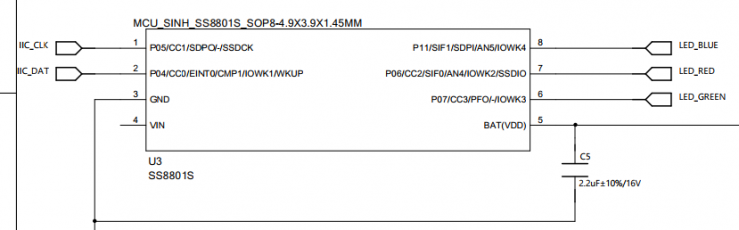
When SS8801 is powered on, P05 is pulled up as I2C Clock and enters SSD mode, resulting in P05 and P06 being unable to be controlled by software. The phenomenon is that P06 cannot control the LED light.
Therefore, because the above factors need to be considered during development, it is necessary to avoid the chip entering the SSD mode by mistake and causing abnormal functions.
Original article, Please mark the attribution when reprinting. SINHMICRO, www.sinhmicro.com.