SS881X chip has two DC5V input pins: VIN and SPWR/VKEY, as shown in the following figure:
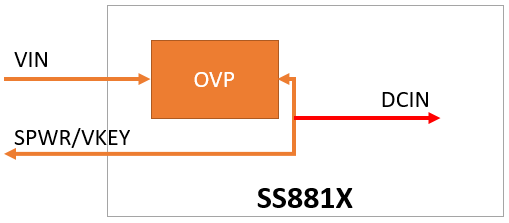
After DC5V is entered through the VIN pin, it will pass through the OVP module and output to the internal DCIN node for use in scenarios such as system power supply and Charger charging.
At the same time, DC5V is input by the VIN pin and can be output by SPWR/VKEY pin to supply for other modules or devices after OVP Protection, In this scenario, SS881X chip can be used as an OVP function to protect devices powered by the SPWR/VKEY pin from the high-voltage pulses generated during the DC5V plugging or pulling out.
In addition, if the DC5V input can be ensured to be safe in the application scenario (no more than 6V), it can directly supply power to other modules or devices through the SPWR/VKEY pin input.
In order to distinguish the two DC5V input paths for the software, SS881X uses the two register state bit (DCINOK and VINOK) to reflect the current input state, and the rules are as follows:
1. Whether DC5V is input from the VIN pin or from the SPWR/VKEY pin, the internal DCIN node are all the 5V input, and DCINOK=1 at this time
2. If DC5V is input from the VIN pin, VINOK=1, otherwise, VINOK=0.
To sum up, it is:
| DCINOK | VINOK | |
| DC5V input from VIN pin | 1 | 1 |
| DC5V input from SPWR/VKEY pin | 1 | 0 |
| DC5V is input from both VIN and SPWR/VKEY | 1 | 1 |
| DC5V is not connected | 0 | 0 |
Original article, Please mark the attribution when reprinting. SINHMICRO, www.sinhmicro.com.